Precision Alignment and Coupling System
Designed for optical-electrical packaging of semiconductor chips, silicon photonic devices, and other passive components, this system provides a highly stable platform for coupling optical fibers (single fiber or FA arrays) with devices such as silicon photonic chips, PLC splitters, AWG arrays, WDM modules, and collimators. It is widely used in both cutting-edge research and industrial production.
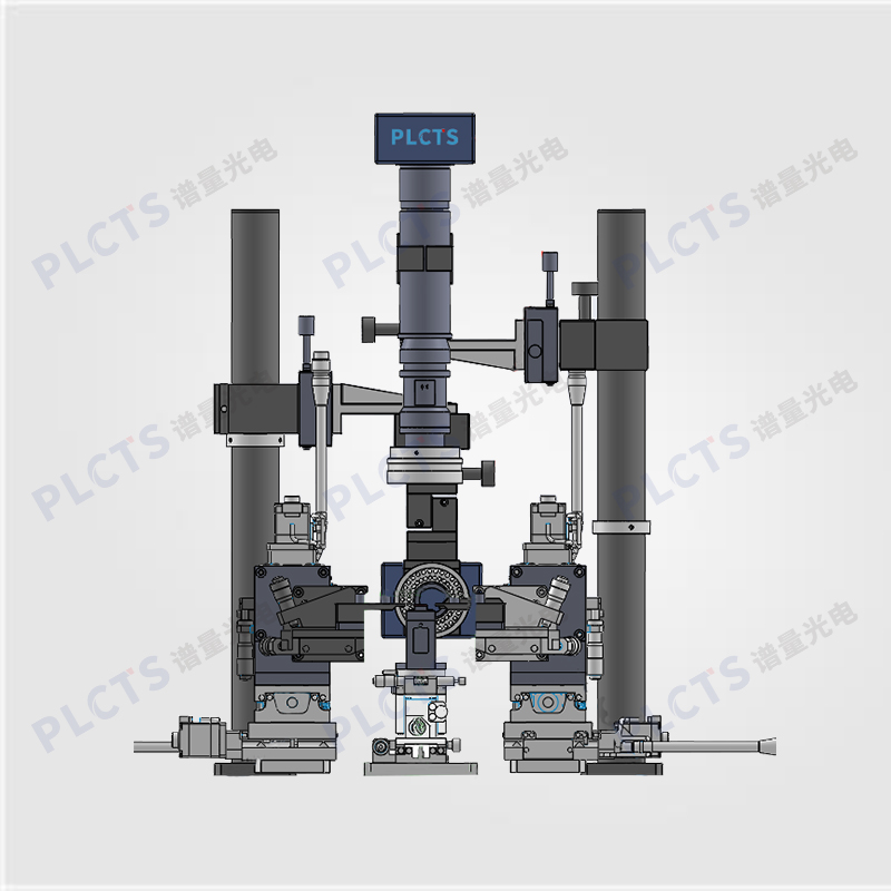
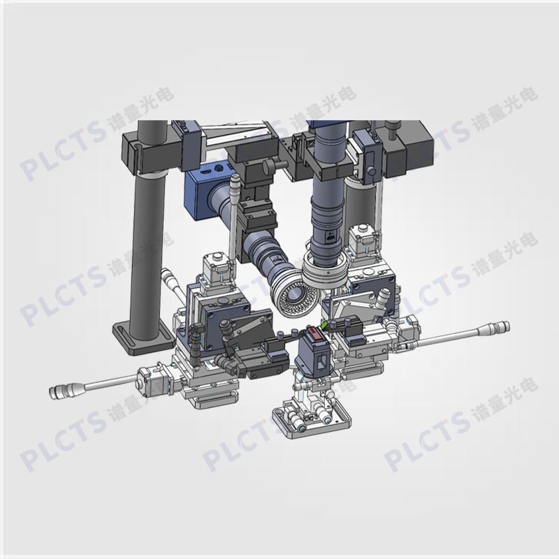
The system integrates precision adjustment stages, device fixtures, a chip stage (with optional temperature control), multi-axis microscope observation modules, light sources, optical platforms, optical power meters, probe holders, and UV curing systems. With comprehensive functionality and user-friendly operation, the system supports custom solutions tailored to specific application needs.
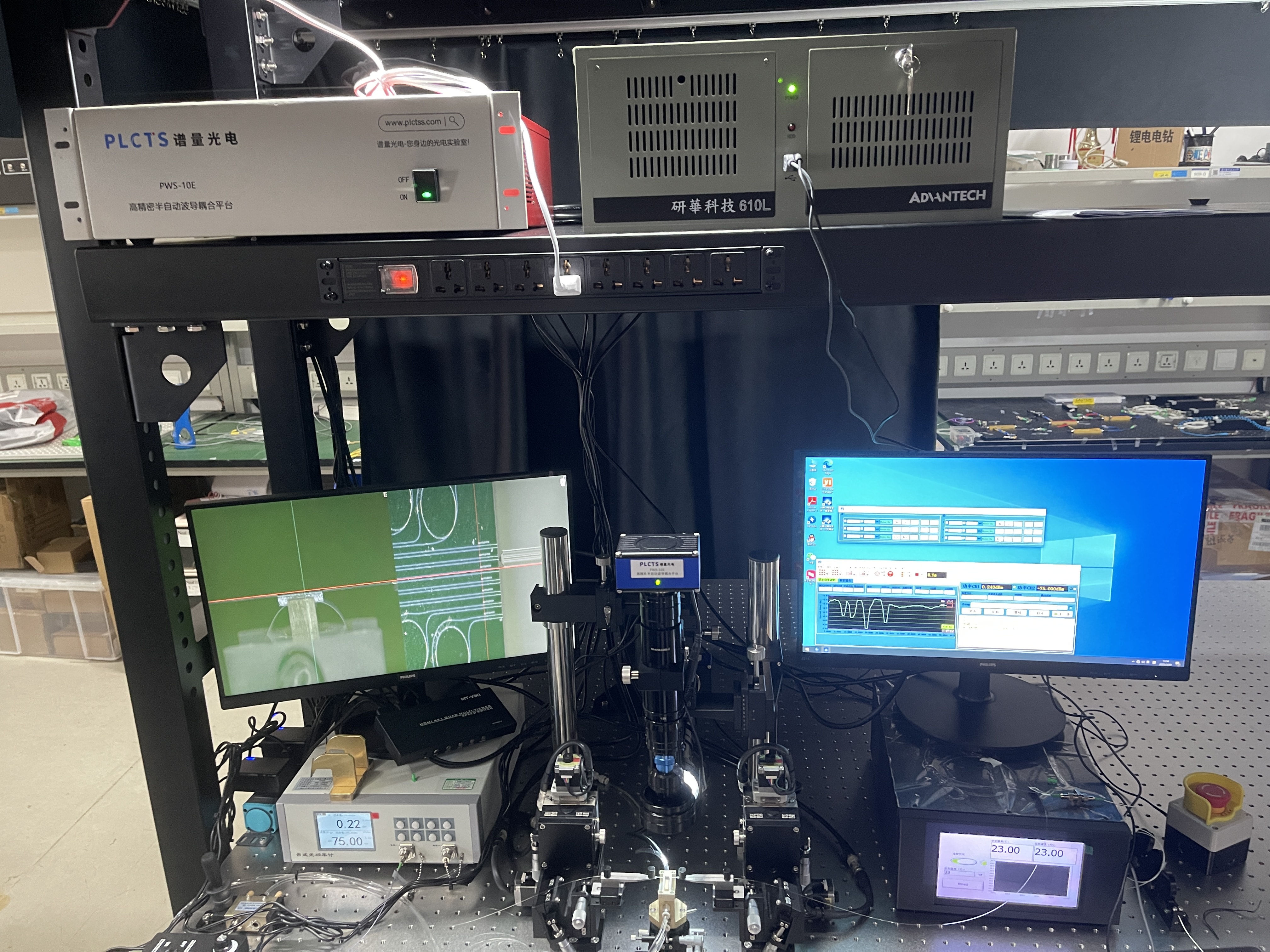
The PWS-10E Series High-Precision Semi-Automatic Waveguide Coupling Platform features dual-side XYZ motorized stages, offering intelligent control, high-precision alignment, and enhanced efficiency. Its modular design allows configuration based on specific application needs, making it an ideal choice for university and institute research. Optional modules such as adhesive dispensing and UV curing are available to support industrial-level coupling and packaging.
Core Modules:
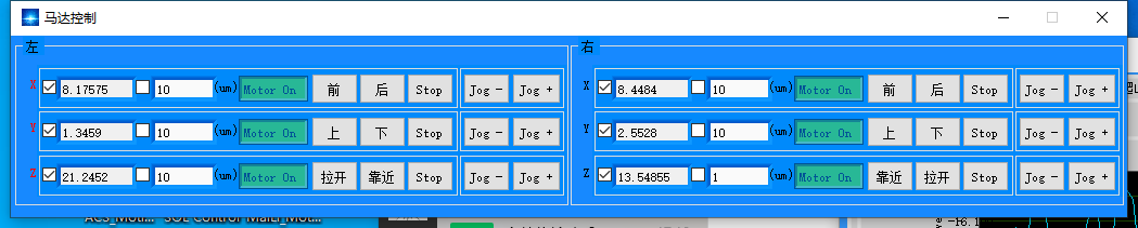
6-DOF Precision Adjustment Stage, XYZ-Axis Motorized Control, and Software Operation for high-accuracy, automated alignment.
Custom fixtures for optical fibers, waveguide chips, etc.
4-axis adjustable chip stage (optional temperature control)
Multi-dimensional microscopic observation system
Supporting components: probe holders, optical platforms, light sources, optical power meters, dispensers, UV curing units, etc.
Technical Advantages:
Modular design, configurable to match specific application needs
Equipp
ed with an imported 6-DOF adjustment stage, featuring 3-axis motorized translation with nanometer-level precision.
User-friendly operation, full workflow completed on a single platform
Broad compatibility, supporting silicon photonics, PLC, AWG, WDM, and more
Custom solutions available based on user requirements
Module Selection & Specifications:
| Module | Model | Qty | Description / Key Specs |
|---|
| 6-Axis Precision Stage | MA-E2000 | 2 | XYZ motorized stage, travel: 20 mm, min step: 0.05 μm, max speed: 20 mm/s, repeatability: ±0.3 μm.
θX/θY resolution: ~0.008°/step, sensitivity: 0.001°. θZ resolution: ~0.009°/step. |
| 6-Axis Controller | TPL26 | 1 | 6-axis integrated motion controller, compatible with dedicated software. |
| Motion Software | SDK-01 | 1 | Includes jog, relative, and scanning modes. Supports step size, speed, and auto loop settings.
With optical power closed-loop optimization and manual/fixed-point mode, supports direct signal peak locking. |
| Custom Fixtures | ALF-D | 1 | For single fibers / FA arrays (horizontal or vertical), PLC, WDM, silicon photonics, etc.
Vacuum or mechanical mounting, TEC compatible. |
| 4-Axis Chip Stage | FDM30 | 1 | X/Y: 13 mm travel, Z: 6 mm, 360° rotation. Integrated imaging system and high-precision manual alignment. |
| Imaging System | LMU-FL | 2/3 | 4D mechanical movement, 86 mm working distance, 2MP digital camera, real-time imaging.
Manual XY travel: 50 mm, resolution: 1 μm. |
| Optical Platform | PLGZT | 1 | Rigid PLGZT platform, customizable size. Optional vibration isolation and light shielding box. |
| Probe Holder | TPLS-UN | 2/4 | With magnetic base, 3-axis manual stage (13 mm travel, 1 μm resolution). Optional: coaxial cable (male), angled tip, or pad alignment. |
| Optional Modules | - | - | ight source, optical power meter, UV curing unit, epoxy dispenser, etc. |
Software Interface:
Optical Device Coupling System↓
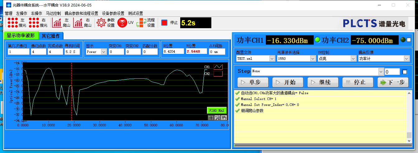
Positioning System↓
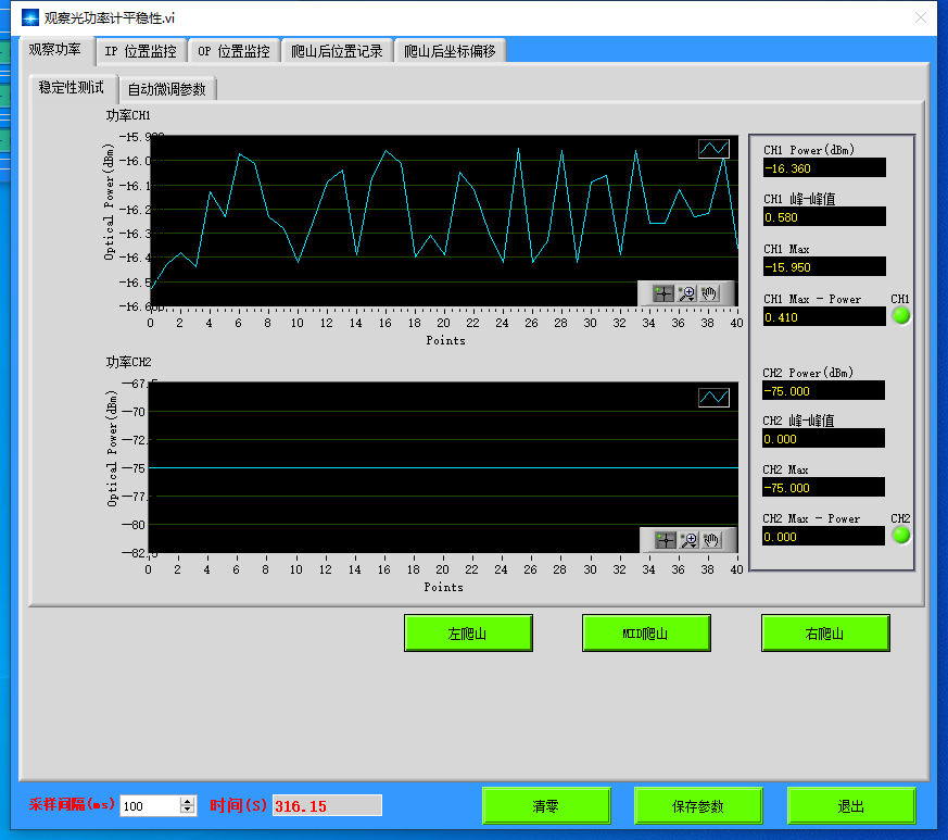
Coupling Feedback (Optical Power Meter)↓
Coupling Workflow
Example: PLC Chip-to-Fiber Alignment
Mechanical Setup:Mount the fiber array and chip on the platform using fixtures. Align each component’s plane and height, ensuring coplanarity and initial positioning accuracy. Fine-tune all axes to minimize angular and positional offsets for optimal coupling.
Initial Optical Alignment:Perform coarse optical alignment along X and Y axes. Use live imaging (overlay of oblique and coaxial views) to assess misalignment. Adjust until the input/output ports of the fiber and chip are well aligned and focused. Light coupling signal appears on the CCD once aligned.
Visual Monitoring:With low-power light coupled into the device, monitor the near-field output (typ. 100–200 μm distance) to evaluate alignment. Adjust rotational angle and height as needed. Use image-based alignment and feedback to iteratively optimize coupling. Fine adjustments are made in ≤10 μm steps.
Signal Optimization:Inject signal light and monitor output power to perform fine tuning. Ensure coupling loss is minimized. Complete alignment of each channel one by one.
UV Curing:Once alignment is complete, apply UV curing to fix the device.
Device Removal:Release the fixture, remove the bonded device, and proceed to testing.
Application fields:
Widely applied in core fields such as scientific research and industrial production. coupling for silicon photonic waveguidesoptical fibers (single fiber / FA arrays)AWGWDMPLCcollimatorscovering a wide range of photonic integration needs.
Project Deliveries:
PLCTS provides customized optical coupling solutions tailored to your specific application needs.For more information, please contact us directly.

 简体中文
简体中文